PI Wagler, Maeke, Tangen BioMIP, RUB
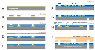
Figure 3: The new modified fabrication process starts with a lithographic step to structure the first conducting layer (Ti/Pt/Au/Ti) containing electrodes, wires and the vias for the upper (2nd) electrode layer (A and B). The following steps (C-E) are a passivation layer (SiO2, 400 nm) deposition and a second Ti/Pt/Au/Ti metallization process and an etching procedure to realize the upper electrodes and wires and to complete via connections. After opening the 2nd passivation layer at the electrode and conducting pad areas I/O holes were placed using deep etching of the silicon substrate by Inductively Coupled Plasma (ICP) to allow a reverse side fluidic connection (F-H). The final steps are soft-lithography fabrication of a PDMS micromoulds, which consist of an array of crossed microfluidic channels as well as bonding the components using oxygen plasma.
