Interaction of porphyrins with pre-structured GaN at room temperature: Multi-STM study
Gallium Nitride (GaN) is a III/IV group, large bandgap semiconductor. Its unique properties, such as high-thermal conductivity, mechanical stability, and mainly direct bandgap of 3.4 eV, makes GaN an important material for numerous applications ranging from light-emitting diodes (LEDs), high-power electronics, and high-temperature operating devices to photocatalysis. However, porphyrins are a remarkable class of metallorganic molecules and a promising candidates to transfer electrons with less energy, efficiently. They are also special to investigate molecular-electronic function due to their robust and tunable proeperties.
GaN is difficult to produce in high quality with bulk crystals under many circumstances. Thus, it is usually developed on Sapphire/Silicon Carbide (SiC) substrates by using the MOVPE (Metalorganic Vapor Phase Epitaxy) technique to optimize the GaN growth in the form of different shapes such as micro-pillars (Fig.1) or nano-rods or only wafers. However, the most crucial problem is their preparation and characterization.
Hence, it is important to know the deficiencies of the fabrication process to find out non ideal behavior of fabricated micro-pillars to resolve the reproducible doping problem. On the other hand, it is also essential to reveal how the inductively-coupled plasma (ICP) etching process affects the epitaxially-grown GaN micro-pillars.
Here, we show how the fabrication deficiencies can be found out by means of atomic scale characterization. Therefore, a Multi-Scale (from 450 µm to nm range) Scanning Tunneling Microscope (STM) is applied at room temperature. Fig. 1 shows the microscopically resolved GaN micro-pillars. Moreover, scanning tunneling spectroscopy (STS) is applied to estimate the bandgap.
Also, this project represents as a second part a molecular study. Porphyrins are adsorbed on GaN micro-pillars. Here, we expect to disclose the important aspects from the point of view of "optimization" of the GaN fabrication process and deposition of porphyrins at semiconducting surface. This will lead to a new realm towards the development of new generation LEDs and solar cells.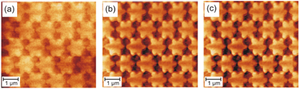
Figure 1: Images recorded during operation of the XYZ-scanning stage based STM.
a) image produced by using the z-signal of the Z-stage of the XYZ-scanning Stage Based STM.
b) Image produced by using the z-signal of the beetle-type STM.
c) Image produced by adding the z- signal of the beetle-type STM and the Z-signal of the Z-stage. The tunneling parameters are: I = 0.153 nA, V = -3.615 V.
Ref.: 1. Kalkan, Fatih. Investigations of GaN-based Micro-pillars by a Multi-scale Scanning Tunneling Microscope. Ph.D. diss., Leibniz University, Hannover, 2012.
Sound interesting? Wanna know more about it?
Please contact: ayub.pathan@rub.de