Scanning Tunneling Microscopy
Scanning tunneling microscopy (STM) was introduced in 1982 by Gerd Binnig and Heinrich Rohrer.1 For this achievement, they were awarded the Nobel Prize in Physics in 1986 shared with Ernst Ruska.
The STM technique allows to probe the electronic structure of a sample. It also yields information on the geometry and on the vibrations of the sample in real space. The principle of STM is based on quantum mechanical tunneling, whereby a tunneling current flows at a small sample-tip distance between a conducting sample and a conducting tip (Fig. 1).
Performing STM measurements:
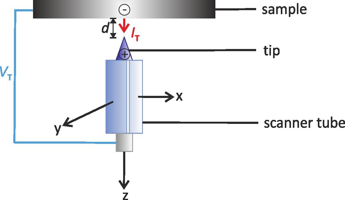
Figure 1: Principle of operation of the STM. To run a STM at constant tunnel current (IT) between sample and tip, a control unit applies a voltage to the piezodrive PZ based on the measured current. Together with the voltages applied to PX and PY for scanning the surface, the applied voltage to piezodrive PZ gives a contour of the constant density of states, which often can be interpreted as the surface topography. Here, only the directions of the piezodrives are shown.
The measurements are usually performed in a constant current mode to probe the electronic structure of the sample. Thereby the tunneling current IT is kept constant during scanning the sample by appropriate voltages applied to piezodrives (see Fig. 1 “scanner tube”) on which e.g. the tip is mounted. One possibility is a scanner tube made of an outer (blue colored) and inner (light gray colored) piezodrive as shown in Fig. 1. These piezodrives are made of piezoelectric ceramics so that a mechanical movement takes place by applying voltages to them. Thus, the tip is moved in x- or y-direction (outer piezodrives Px and Py ) or in z-direction (inner piezodrive PZ ). Simultaneously a feedback loop controls the distance between the sample and the tip d to achieve a constant tunneling current. Finally, the applied voltages to all piezodrives are converted into a topographic image of the explored surface.
STM tip and STM images:
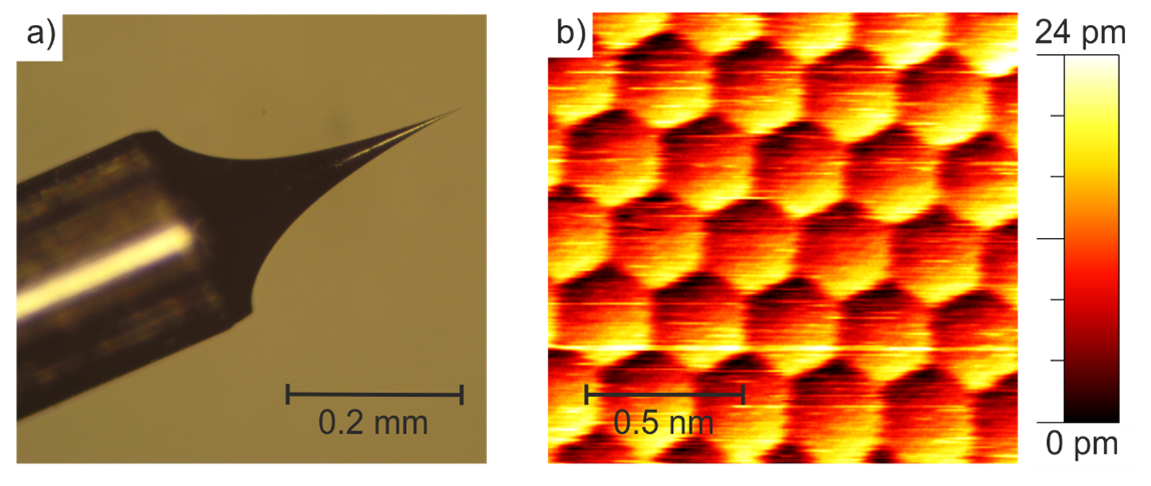
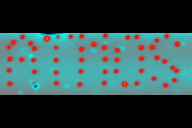
Figure 2: (a) Optical microscope image of a freshly-etched tungsten tip. (b) STM image of the atoms of the Au(111) surface (-61 mV, 1430 nA).
Usually, a tip made of tungsten or of platinum-iridium is used for STM measurements. In Fig. 2 a, a freshly-etched tungsten tip is shown. With such a good tip, it is possible to measure images with an atomic resolution, like the one shown in Fig. 2 b.
Quantum mechanical tunneling:
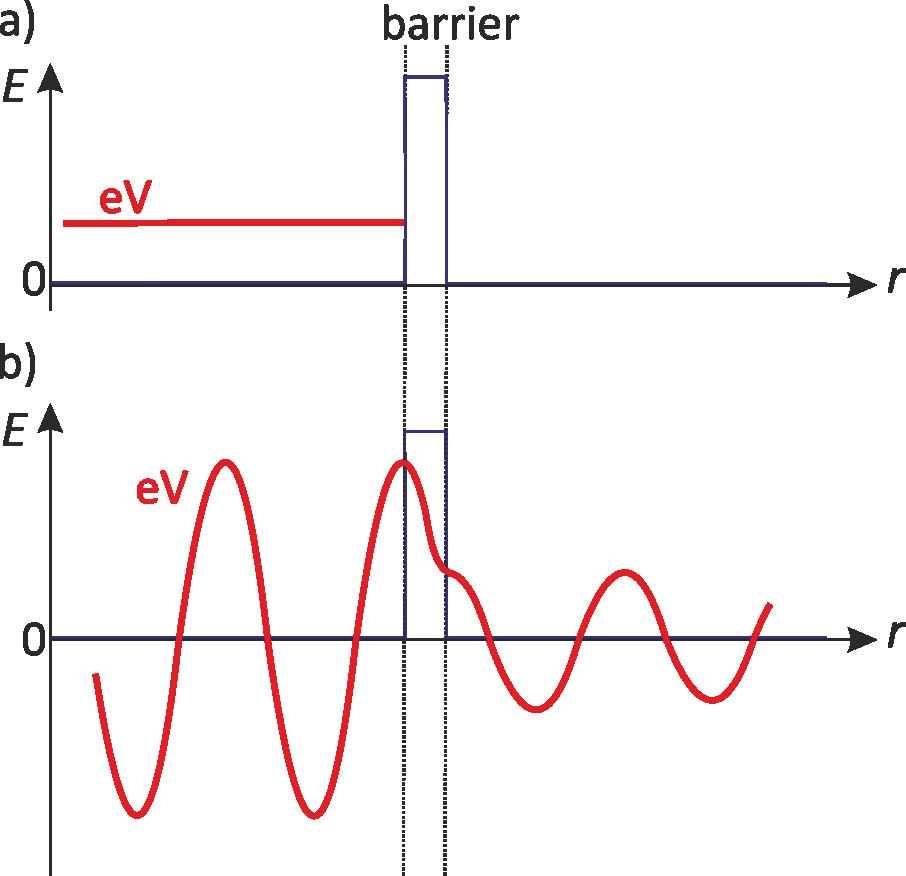
Figure 3: The propagation of an electron through a potential barrier with higher energy than its own energy in a) classical mechanics, whereby the electron does not propagate and in b) quantum mechanics, whereby a part of the wave propagates through the potential energy barrier.
In classical mechanics, it is not possible for a particle to pass a barrier, if the energy (E) of the particle is smaller than the potential energy (EP) of the barrier (see Fig. 3 a). In quantum mechanics it works! The particle in quantum mechanics, here the electron, has particle-like properties as well as wave-like properties. If the potential energy barrier is thin enough, the electron can pass the barrier (see Fig. 3 b). The nature of a wave to propagate through a potential energy barrier with lower energy than the energy of the potential barrier is called quantum mechanical tunneling.
Quantum mechanics applied to STM:
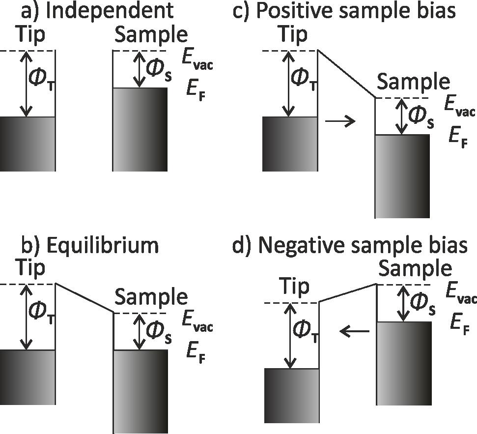
Figure 4: Energy band diagrams for the STM tip and sample: (a) not interacting tip and sample and equivalent vacuum level Evac. (b) At a small distance between tip and sample the Fermi levels EF align. (c) With a positive voltage applied to the sample, the electrons tunnel from filled tip states into empty sample states. (d) with negative voltage applied to the sample, the electrons tunnel from filled sample states to empty tip states. The arrows in (c) and in (d) show the direction of the electron flux.
In STM experiments the potential energy barrier is a small vacuum gap of tenth of nanometers between the sample and the tip. Both the electrons of the sample and tip have their own highest energy level at which the electrons sit, the so called Fermi level EF, and their own energy to overcome the potential energy barrier, the so called work function Φ (Fig. 4 a). At a sufficiently small distance d between sample and tip the Fermi levels of tip and sample align due to tunneling (Fig. 4 b). Application of an electric voltage between the sample and the tip at this small distance, lowers the Fermi level of the sample (Fig. 4 c) or of the tip (Fig. 4 d) by the bias applied and a tunneling current IT from the sample to the tip flows (compare Fig. 1). Crucial is hereby that both, the tip and the sample are conductive.
The tunneling current depends exponentially on the distance d between tip and sample and a constant κ, whereby κ depends on the average work function Φ0 of sample and tip and the mass of an electron m:2
For more details see Morgenstern et al. 2013.3
1 G. Binnig, and H. Rohrer (1982): Scanning tunneling microscopy. Helv. Phys. Acta 55 (6), pp. 726–735.
2 G. Binnig, H. Rohrer, Ch. Gerber, and E. Weibel (1982): Surface Studies by Scanning Tunneling Microscopy. Phys. Rew. Lett. 49 (1), pp. 57–61.
3 K. Morgenstern, N. Lorente, and K.-H. Rieder (2013): Controlled manipulation of single atoms and small molecules using scanning tunneling microscope. Phys. Status Solidi B (9), pp. 1671-1751.
Controlled manipulation of single atoms and small molecules using the scanning tunnelling microscope
This article reviews manipulation of single molecules by
scanning tunnelling microscopes, in particular vertical manip-
ulation, lateral manipulation, and inelastic electron tunnelling
(IET) manipulation.