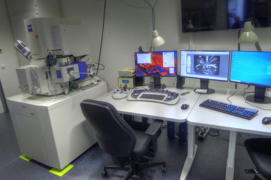
Zeiss Merlin FE-SEM
Our lab uses a Merlin FE-SEM manufactured by Zeiss.
Scanning electron microscopy (SEM) is predominantly used to image smallest things. Spatial resolution down to the submicrometer scale is a standard operation mode. The high-resolution field emission SEM is equipped with an EDX detector to analyse the elemental composition of a sample. With an EBSD detector we can analyse the specific crystal orientation of geological or metallurgical samples.

HR-FESEM Zeiss Merlin Gemini II
- Manufacturer: Zeiss
- Model: Merlin, Gemini II
Electron column
- Electron source: thermic Schottky field emitter (beam current stability better than 0.2% / hour)
- Acceleration voltage: 0.1 – 20/30 kV
- Resolution: 0.8 nm at 15kV, 1.4 nm at 1kV (at 40 nA configuration)
Detectors
- Everhardt-Thornley detector for secondary electrons (chamber detector)
- Inlens detector for secondary electrons
- Backscatter electron detector BSD4 (chamber detector)
- Inlens: Energy selective backscattered detector (EsB)
- EDX silicon drift detector N-Max (150 mm2), Oxford Instruments (127 eV energy resolution)
- EBSD detector Nordlys equipped with two forescatter diodes (Oxford Instruments, 0.1° angular resolution)
Vacuum system
- Edwards scrollpump nXDS15i
- Turbomolecular pump
- Ion getter pumps - two for the gun vacuum
Additional features
- Gas Injection System for charge compensation
- Plasma cleaner
- Small specimen chamber (quick specimen exchange)
- Super-eucentric stage with six-axes
- Chamber scope
Periphery
- EDX/EBSD Aztec Crystal 4.3 software package
- Control PC online for EDX/EBSD
- Analysis PC offline for EDX/EBSD
- Link Box controlling the forescatter diodes
- Water chiller

